

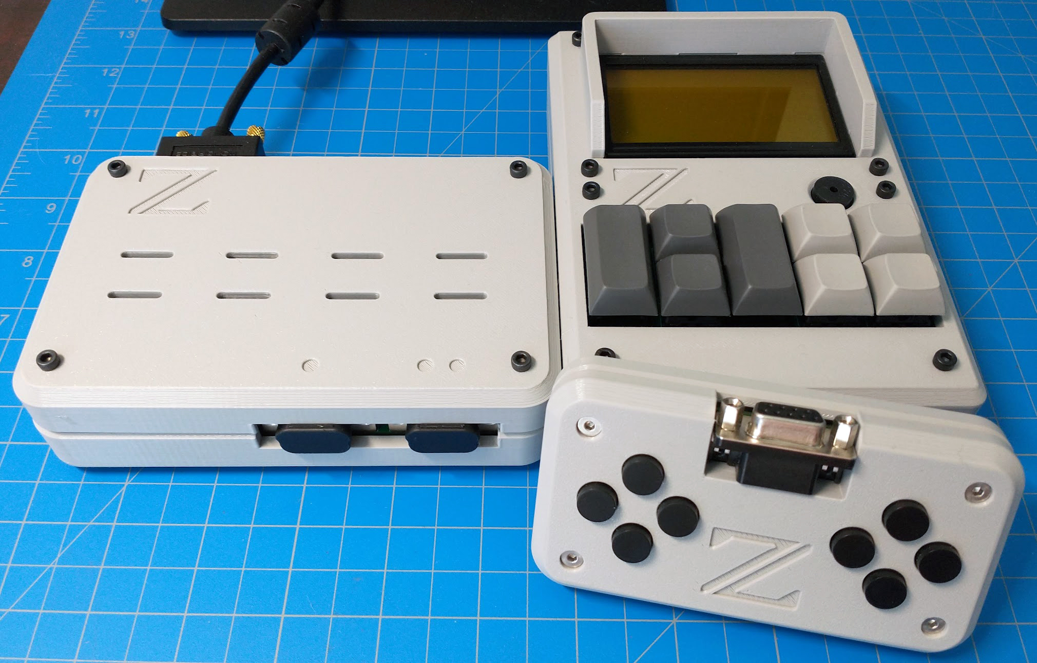
Z-FIGHTER's VGA module outputs an industry standard 640x480 signal at 60 Hz. Its design is based around TTL logic chips (counters, buffers, support logic) and two programmable GAL chips. 1536 bytes of addressable VRAM are scaled up 4X to produce a chunky monochrome 128x96 pixel image, emphasizing compatibility with programs intended for Z-FIGHTER's 128x64 ST7920 LCD and supporting an additional 32 pixels of vertical resolution for programs targeting the VGA module. All VRAM writes from Z-FIGHTER occur without interrupting or interfering with the output video signal. Two DE-9 "joystick" ports are provided to the user allowing the sampling of 8 joystick buttons or one byte of data from alternative devices (analog-to-digital converted sensors, potentiometers, etc.) per port. A 3-position DIP switch is connected across the red, green and blue VGA signals allowing a crude means to change the output video color. Lastly, a jumper-selectable 60 Hz interrupt generator is provided to act as an optional timebase for Z-FIGHTER software.
Since designing Z-FIGHTER's expansion port around an Intel 8255 Programmable Peripheral Interface (PPI) IC, I've felt some anxiety around what could potentially be achieved with it. Certainly, it's very convenient to have an easily programmable parallel port to interface with all sorts of devices without needing any additional address decoding, but without full exposure of the system's address and data lines it's not possible to place additional memory within Z-FIGHTER's memory map. As a result, when intending to implement some sort of video RAM, memory writes must be performed with I/O instructions instead of directly interfacing with the CPU. There is a precedent for such a scheme, most notably in my mind being the MSX architecture's TMS9918 VDP and its subsequent iterations. With that in mind, I decided to dive into my first experience with analog video design.
I began this project by creating a Circuit JS simulation (download below). This came very much in handy when designing the circuit and was very helpful when writing the GAL equations which decode the CD74HC4040 counters responsible for synchronization and producing the SRAM control signals.
The VGA module takes advantage of all three 8255 PPI ports. A data byte and the destination address (0h to 05FFh) are placed in parallel across 19 PPI I/O pins before a single 'write ready' control signal is pulsed to complete a write cycle. This allows for a reasonably tight loop when performing VRAM writes. In its current implementation, a 128x64 bitmap (1024 bytes) can be pushed to the VGA module's VRAM in approximately 16.2 ms. At this speed, it's quite practical to simply maintain a copy of the screen data in system RAM and push full frames to the VGA module when necessary, but programs that directly address VRAM for maximum efficiency are entirely possible.
PUBLIC _vga
_vga:
	LD      A,80h
	OUT     (CTRL),A    ; Initialize PPI
	LD      DE,0        ; Initialize destination address
	LD      BC,1536     ; Initialize byte counter
LOOP:
	LD      A,(HL)      ; Load byte in (HL) to port A
	OUT     (PORTA),A

	LD      A,E         ; Load lower destination address to port B
	OUT     (PORTB),A

	LD      A,D         ; Load upper destination address to port C
	OUT     (PORTC),A

	LD      A,7         ; Toggle WRDY ("write ready" control signal)
	OUT     (CTRL),A
	DEC     A
	OUT     (CTRL),A

	INC     HL
	INC     DE

	DEC     BC          ; Check byte counter
	LD      A,C
	OR      B
	JP      NZ,LOOP     ; Repeat until last byte is written

	RET
Because Z-FIGHTER's expansion port has its /INT line exposed to peripherals, it seemed appropriate to provide an optional 60 Hz interrupt to the system for timekeeping and display synchronization.
While designing the VGA module, it hadn't occurred to me that the Z80's /INT pin is level-sensitive (as opposed to being negative edge-triggered like the /NMI pin). If the /INT line is held low longer than an interrupt service routine (ISR) takes to execute, maskable interrupts will continuously retrigger until the /INT pin is no longer active. On the other hand, an /INT pulse should be longer than the slowest Z80 instruction (23 t-states) to ensure it is always caught by the CPU. I determined that a pulse longer than 3.12 microseconds was appropriate for Z-FIGHTER's CPU clock frequency. In testing, pulses 10 microseconds and longer began to cause retriggering with a minimal ISR.
To satisfy these requirements and provide a useful interrupt, the VGA module generates an interrupt pulse for a duration of 128 VGA 'pixels' shortly after the contents of the VRAM have been output to the screen. I was encouraged by the fact that my implementation is somewhat similar to the ZX Spectrum's vertical blanking interrupt. Of course, with a more robust solution that allowed the system to acknowledge and release an interrupt, such careful timing wouldn't be necessary!
I found the 74HC541 buffers used heavily in this design to be particularly problematic while this project was still implemented on a breadboard, resulting in noise and invalid addressing when performing VRAM writes and inconsistent behavior when sampling input from controllers. Despite these issues, I chose to move forward with committing the design to a PCB. After assembling a prototype, all issues with the buffers had completely vanished.
A persistent issue was some interference caused by an active-low /LD pulse generated every 32 'VGA' pixels when loading a VRAM byte into the 74HC165 shift register used for video output. After some trial and error, the visual artifacts were cleaned up by connecting the '165's QH and CLK pins to GND with 470 pF capacitors.
Video of the VGA module prototype running Z-FIGHTER's video poker game
(MP4, 1.65 MB)
Download
Test of interrupt-driven graphics (scrolling line at 60 Hz)
(MP4, 21.2 MB)
Download
Simulation file for loading into Circuit JS (TXT, 12 KB)
Download
Preview